Micron targets 42 Gb/mm2 density for G11 NAND in late 2027
The company plans to double storage density and boost I/O speeds by 50 percent using wafer-on-wafer bonding technology.
By Priya Sharma ·
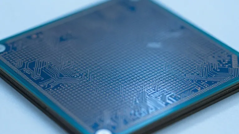
Micron announced this week that its next generation of 3D NAND flash, designated G11, will enter high-volume production in the second half of 2027. The update follows the company's current G9 architecture and aims to address growing demands for higher bandwidth and energy efficiency in both client and data center environments.
Storage density is expected to double from approximately 21 Gb/mm2 to 42 Gb/mm2 in triple-level-cell form. This increase is intended to outpace next-generation products from competitors Kioxia and Samsung, which are currently developing their own advanced memory solutions.
Performance metrics will also see substantial changes. Input/output speeds are projected to rise by up to 50 percent, moving from 3,600 MT/s to 5,400 MT/s. Simultaneously, the energy required to transfer each bit should decrease by more than 25 percent, a metric critical for artificial intelligence workloads that require sustained high throughput.
A primary technical shift in the G11 design is the adoption of wafer-on-wafer bonding. This method allows the memory array and peripheral circuitry to be manufactured on separate wafers using optimized processes before being bonded together. Scott DeBoer, Micron's president and chief technology and products officer, confirmed the use of this technique, stating, "This is the right timing for that technology." He described G11 as the world's most advanced NAND.
The new architecture will exceed 400 layers, though Micron has not yet disclosed the exact number of active wordlines or memory decks. The company attributes the density gain to a combination of increased layer counts and smaller memory cell dimensions. Further technical details are scheduled for release in 2027 as production ramps up.
Looking beyond the G11 generation, Micron plans to continue scaling in all three dimensions rather than relying solely on layer count. DeBoer noted that the company is developing high-mobility materials and ultra-dense cell architectures to improve transistor characteristics and reduce internal data movement energy. No specific production schedules or density targets for generations following G11 have been disclosed.
Source: Tom's Hardware